(China (Mainland))

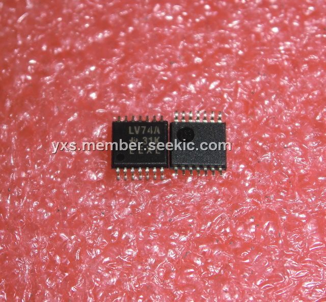
Product Summary
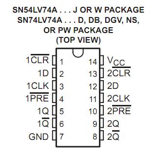
The LV74A is a dual positive-edge-triggered D-type flip-flop designed for 2-V to 5.5-V VCC operation. A low level at the preset (PRE) or clear (CLR) inputs sets or resets the outputs, regardless of the levels of the other inputs. When PRE and CLR are inactive (high), data at the data (D) inputs meeting the setup-time requirements is transferred to the outputs on the positive-going edge of the clock pulse. Clock triggering occurs at a voltage level and is not directly related to the rise time of the clock pulse. Following the hold-time interval, data at the D input can be changed without affecting the levels at the outputs. The LV74A is fully specified for partial-power-down applications using Ioff. The Ioff circuitry disables the outputs, preventing damaging current backflow through the devices when they are powered down.
Parametrics
LV74A absolute maximum ratings: (1)Supply voltage range, VCC: -0.5 V to 7 V; (2)Input voltage range, VI: -0.5 V to 7 V; (3)Voltage range applied to any output in the high-impedance or power-off state, VO:- 0.5 V to 7 V; (4)Output voltage range, VO: -0.5 V to VCC + 0.5 V; (5)Input clamp current, IIK (VI < 0): -20 mA; (6)Output clamp current, IOK (VO < 0): -50 mA; (7)Continuous output current, IO (VO = 0 to VCC) ±25 mA; (8)Continuous current through VCC or GND ±50 mA.
Features
LV74A features: (1)2-V to 5.5-V VCC Operation; (2)Max tpd of 8.5 ns at 5 V; (3)Typical VOLP (Output Ground Bounce)<0.8 V at VCC = 3.3 V, TA = 25℃; (4)Typical VOHV (Output VOH Undershoot)>2.3 V at VCC = 3.3 V, TA = 25℃; (5)Support Mixed-Mode Voltage Operation on All Ports; (6)Ioff Supports Partial-Power-Down Mode peration; (7)Latch-Up Performance Exceeds 250 mA Per JESD 17; (8)ESD Protection Exceeds JESD 22.
Diagrams